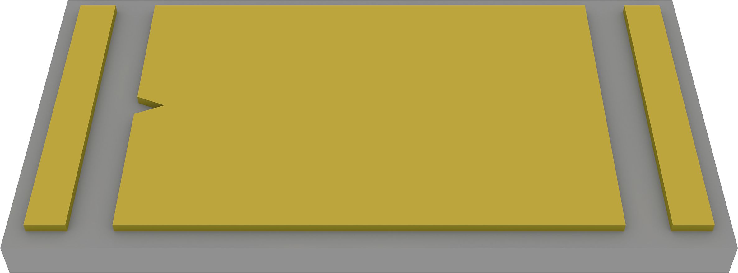
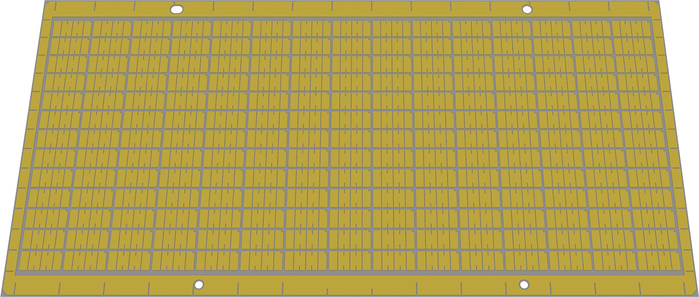
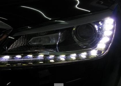
Thin-film circuit ceramic packaging substrates are widely used in 5G optoelectronic devices such as LED lighting, UV LED, car lights, flashlights, face recognition, and Lidar due to their high reliability, high thermal conductivity, high circuit resolution, high circuit flatness.

Features: This substrate features the surface of the product is flat, the chip can be closely attached to the substrate, the cavity rate is low, suitable for the packaging of flip chip.
Model:
7035Material:
aluminum nitrideSubstrate Thickness:
0.51±0.05 mmNumber Of Typeset:
168 pcs/sheetSheet Size:
109.2×54.5 mmSingle Size:
7.0×3.5 mmMinimum Line Width:
0.8 mmGap Size:
0.13 mmMinimum Aperture:
0.07 mmCopper Thickness:
65±15 μmDam Thickness:
Step Height:
Boss Copper Thickness:
Metal Column High: