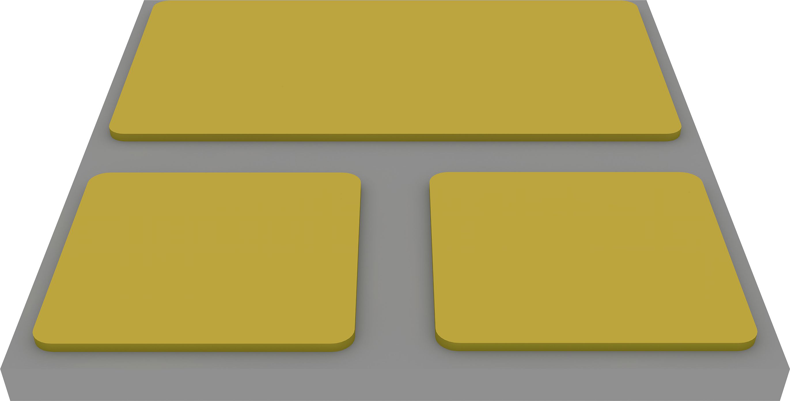
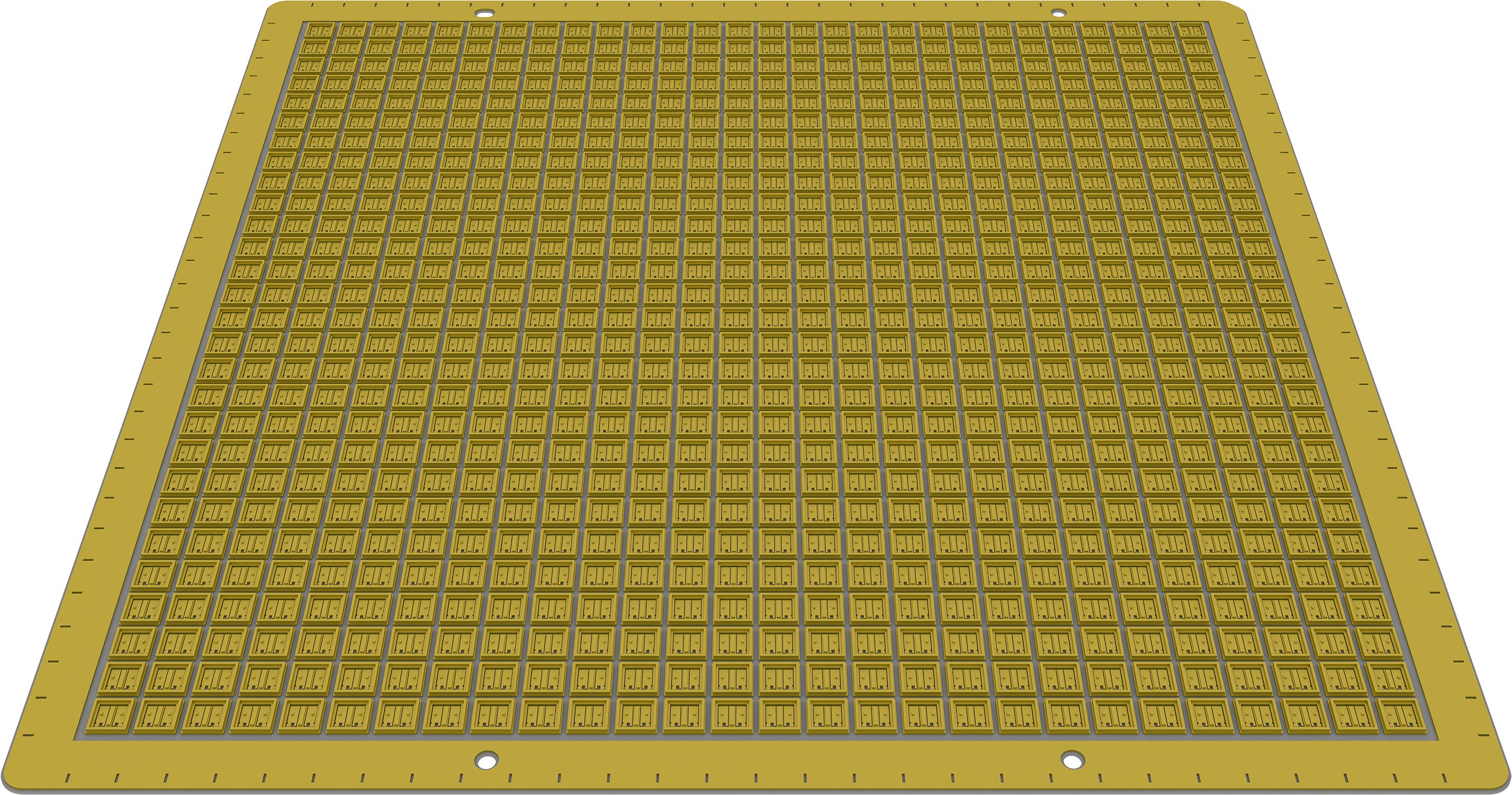
Thin-film circuit ceramic packaging substrates are widely used in 5G RF front-end discrete devices and module packaging due to their high reliability, high thermal conductivity, high circuit resolution, high circuit flatness, and excellent noise reduction and anti-interference capabilities.

Features: This substrate features high line flatness and high line resolution, and produced with a highly controllable boss design and a shielding cavity design, suitable for the CSP packaging of duplexer.
Model:
3535Material:
Alumina/aluminum nitrideSubstrate Thickness:
1.1±0.15 mmNumber Of Typeset:
784 pcs/sheetSheet Size:
109.2×109.2 mmSingle Size:
3.34×3.34 mmMinimum Line Width:
0.14 mmGap Size:
0.07 mmMinimum Aperture:
0.07 mmCopper Thickness:
50±15 μmDam Thickness:
400±50 μmStep Height:
40±15 μmBoss Copper Thickness:
40±15 μmMetal Column High: