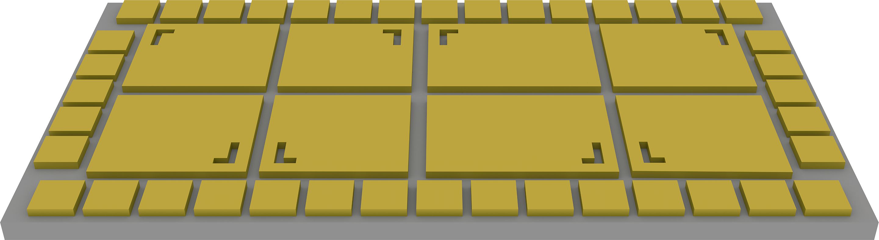
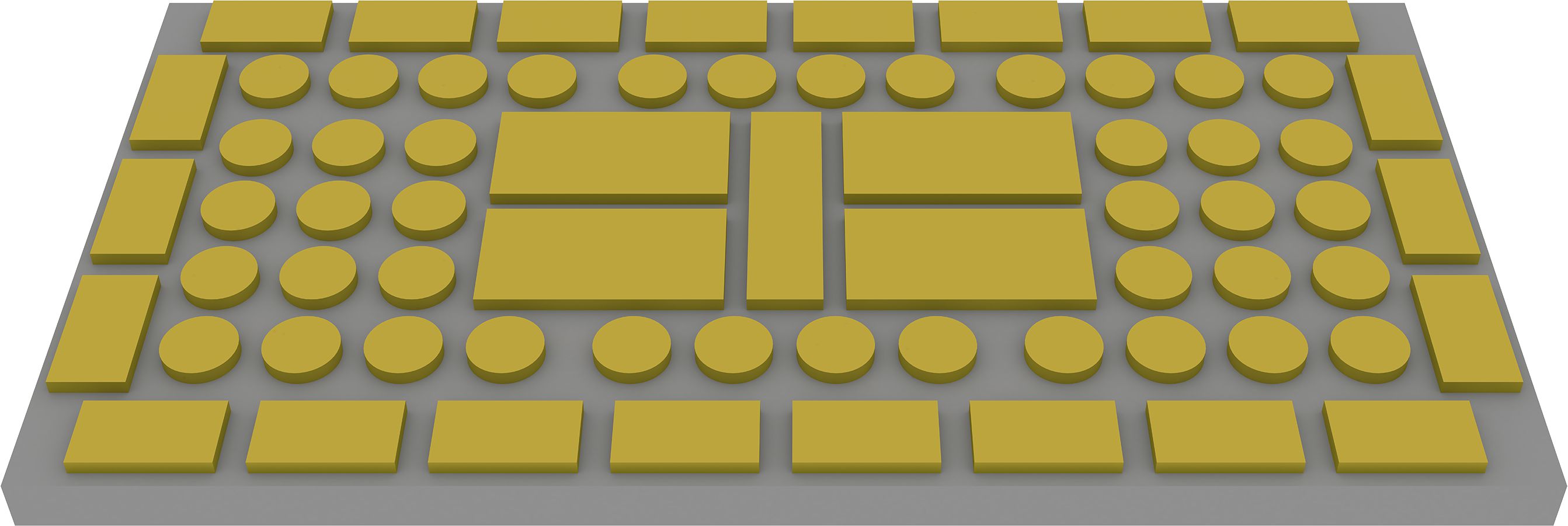
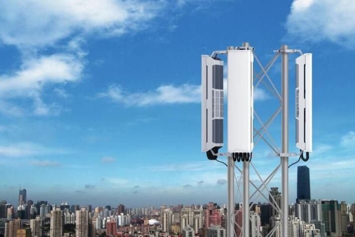
Thin-film circuit ceramic packaging substrates are widely used in 5G RF front-end discrete devices and module packaging due to their high reliability, high thermal conductivity, high circuit resolution, high circuit flatness, and excellent noise reduction and anti-interference capabilities.

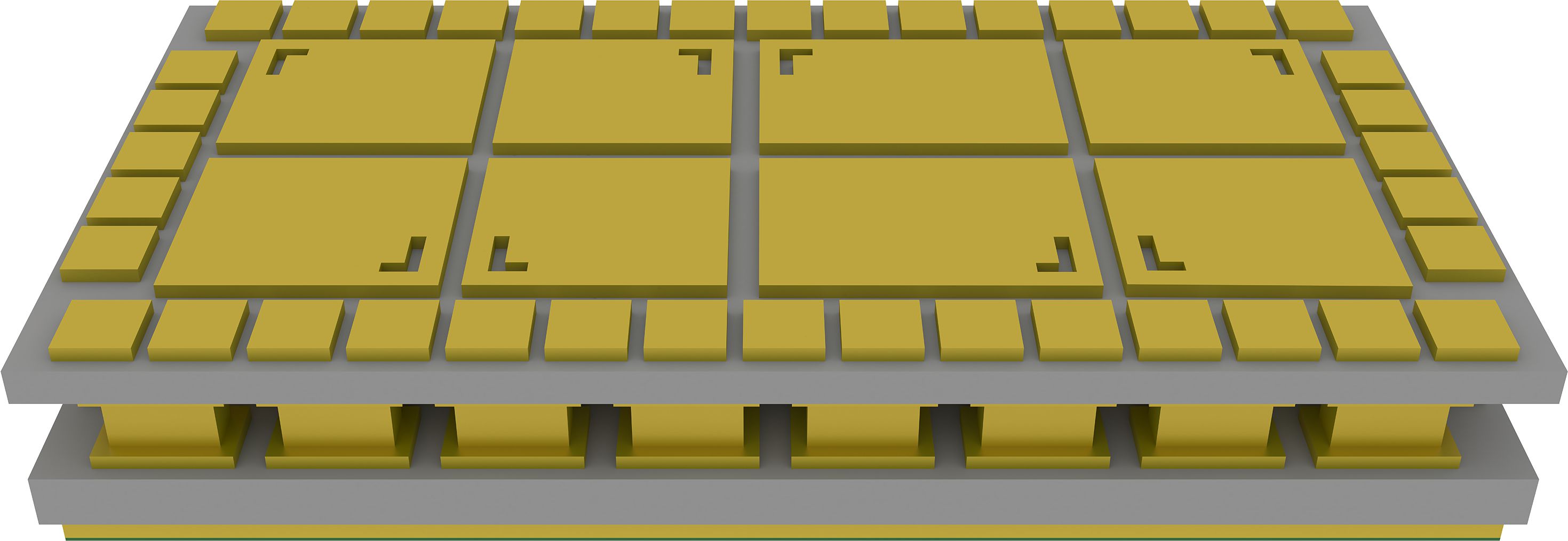
Features: This substrate has a high degree of integration, high reliability, and low cost. It is also miniaturized, allowing it to realize the 3D packaging of upper and lower RF modules with different functions along the vertical direction.
Model:
9550Material:
Alumina/aluminum nitrideSubstrate Thickness:
0.69±0.15 mmNumber Of Typeset:
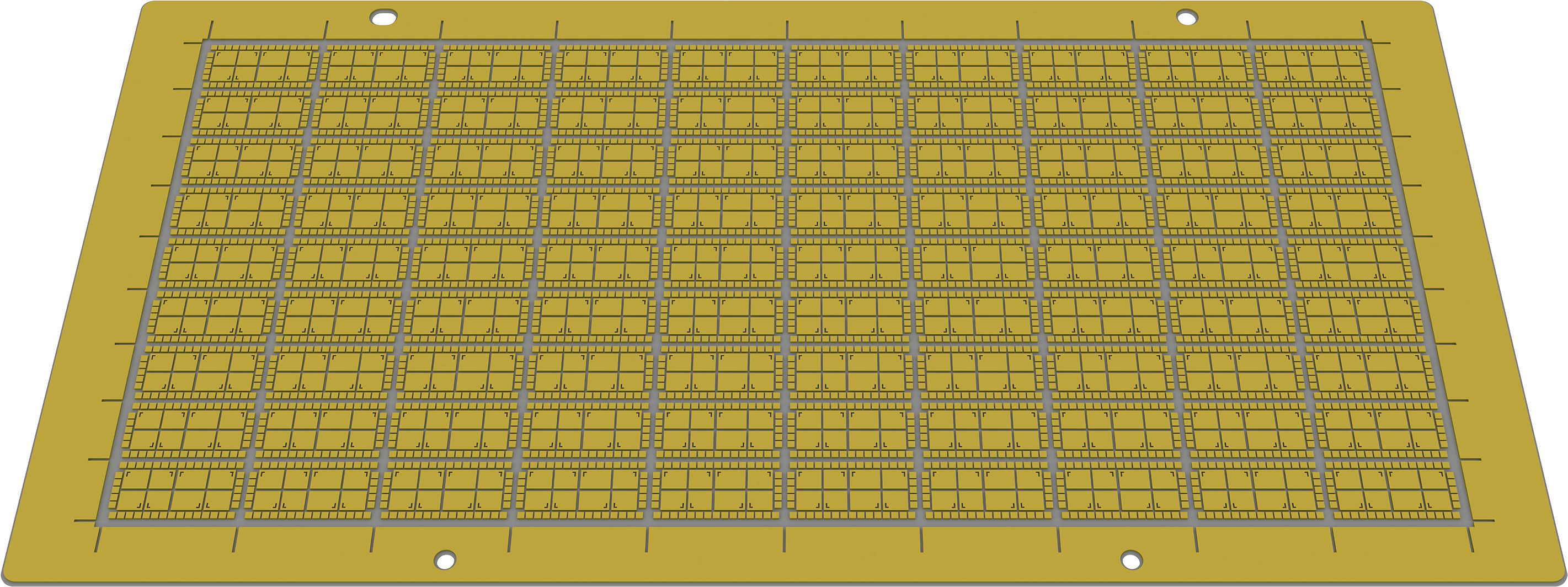
90 pcs/sheetSheet Size:
109.2×54.5 mmSingle Size:
9.45×4.76 mmMinimum Line Width:
0.13 mmGap Size:
0.15 mmMinimum Aperture:
0.07 mmCopper Thickness:
65±15 μmDam Thickness:
Step Height:
Boss Copper Thickness:
Metal Column High:
400±50 μm